 | –≠–ª–µ–∫—Ç—Ä–æ–Ω–Ω—ã–π –∫–æ–º–ø–æ–Ω–µ–Ω—Ç: MAX1121 | –°–∫–∞—á–∞—Ç—å:  PDF PDF  ZIP ZIP |
General Description
The MAX1213 is a monolithic, 12-bit, 170Msps analog-
to-digital converter (ADC) optimized for outstanding
dynamic performance at high-IF frequencies up to
300MHz. The product operates with conversion rates
up to 170Msps while consuming only 788mW.
At 170Msps and an input frequency up to 250MHz, the
MAX1213 achieves a spurious-free dynamic range
(SFDR) of 72.9dBc. Its excellent signal-to-noise ratio
(SNR) of 65.8dB at 10MHz remains flat (within 2dB) for
input tones up to 250MHz. This ADC yields an excellent
low-noise floor of -68dBFS, which makes it ideal for
wideband applications such as cable head-end
receivers and power-amplifier predistortion in cellular
base-station transceivers.
The MAX1213 requires a single 1.8V supply. The analog
input is designed for either differential or single-ended
operation and can be AC- or DC-coupled. The ADC also
features a selectable on-chip divide-by-2 clock circuit,
which allows the user to apply clock frequencies as high
as 340MHz. This helps to reduce the phase noise of the
input clock source. A low-voltage differential signal
(LVDS) sampling clock is recommended for best perfor-
mance. The converter's digital outputs are LVDS com-
patible and the data format can be selected to be either
two's complement or offset binary.
The MAX1213 is available in a 68-pin QFN package
with exposed paddle (EP) and is specified over the
industrial (-40∞C to +85∞C) temperature range.
See the Pin-Compatible Versions table for a complete
selection of 8-bit, 10-bit, and 12-bit high-speed ADCs in
this family.
Applications
Base-Station Power-Amplifier Linearization
Cable Head-End Receivers
Wireless and Wired Broadband Communication
Communications Test Equipment
Radar and Satellite Subsystems
Features
o 170Msps Conversion Rate
o Low Noise Floor of -68dBFS
o Excellent Low-Noise Characteristics
SNR = 65.8dB at f
IN
= 65MHz
SNR = 64.5dB at f
IN
= 250MHz
o Excellent Dynamic Range
SFDR = 76.5dBc at f
IN
= 65MHz
SFDR = 72.9dBc at f
IN
= 250MHz
o 59.5dB NPR for f
NOTCH
= 28.8MHz and a Noise
Bandwidth of 50MHz
o Single 1.8V Supply
o 788mW Power Dissipation at f
SAMPLE
= 170MHz
and f
IN
= 65MHz
o On-Chip Track-and-Hold Amplifier
o Internal 1.23V-Bandgap Reference
o On-Chip Selectable Divide-by-2 Clock Input
o LVDS Digital Outputs with Data Clock Output
o MAX1213 EV Kit Available
MAX1213
1.8V, 12-Bit, 170Msps ADC for
Broadband Applications
________________________________________________________________ Maxim Integrated Products
1
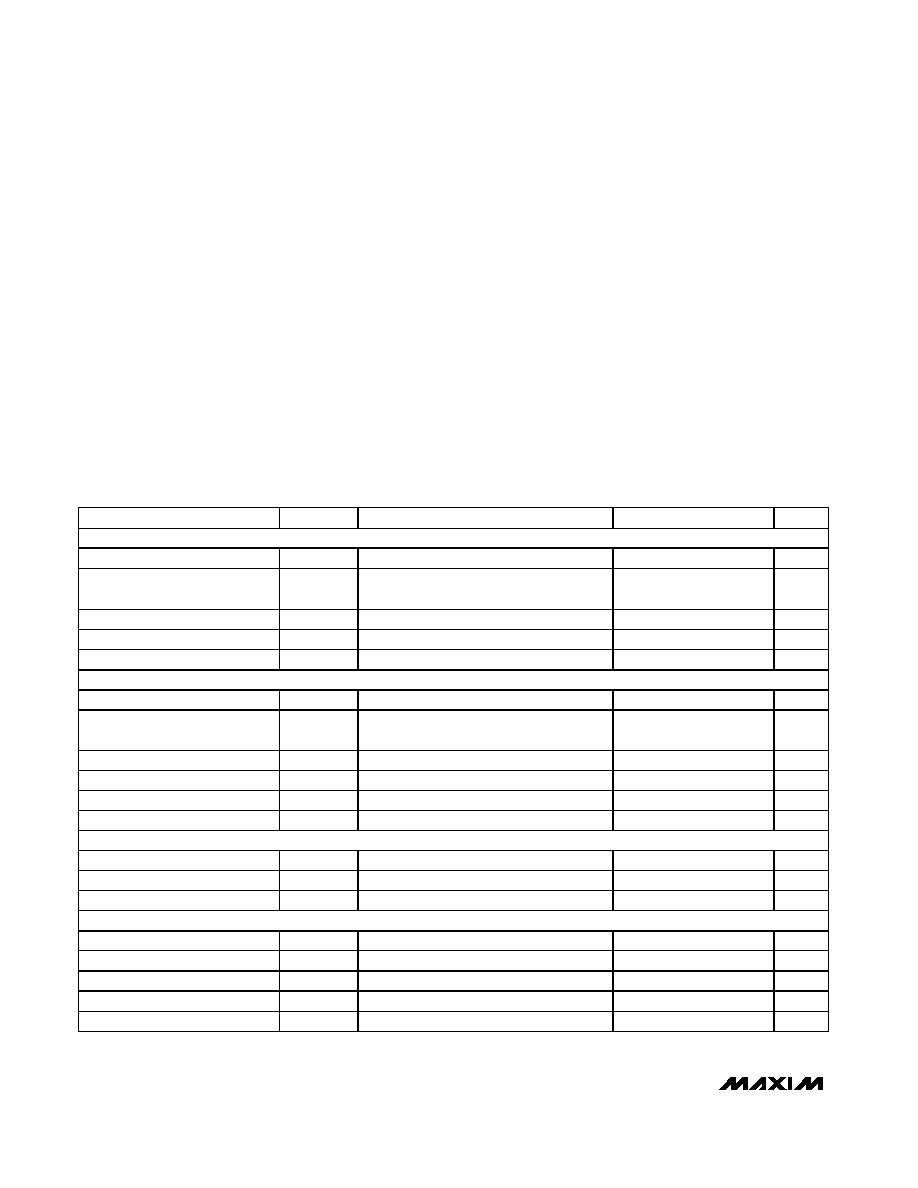
PART
TEMP RANGE
PIN-PACKAGE
MAX1213EGK
-40
∞C to +85∞C
68 QFN-EP*
Ordering Information
19-1003; Rev 2; 6/05
For pricing, delivery, and ordering information, please contact Maxim/Dallas Direct! at
1-888-629-4642, or visit Maxim's website at www.maxim-ic.com.
*EP = Exposed paddle.
EVALUATION KIT
AVAILABLE
Pin-Compatible Versions
PART
RESOLUTION
(BITS)
SPEED GRADE
(Msps)
MAX1121
8
250
MAX1122
10
170
MAX1123
10
210
MAX1124
10
250
MAX1213
12
170
MAX1214
12
210
MAX1215
12
250
Pin Configuration appears at end of data sheet.
MAX1213
1.8V, 12-Bit, 170Msps ADC for
Broadband Applications
2
_______________________________________________________________________________________
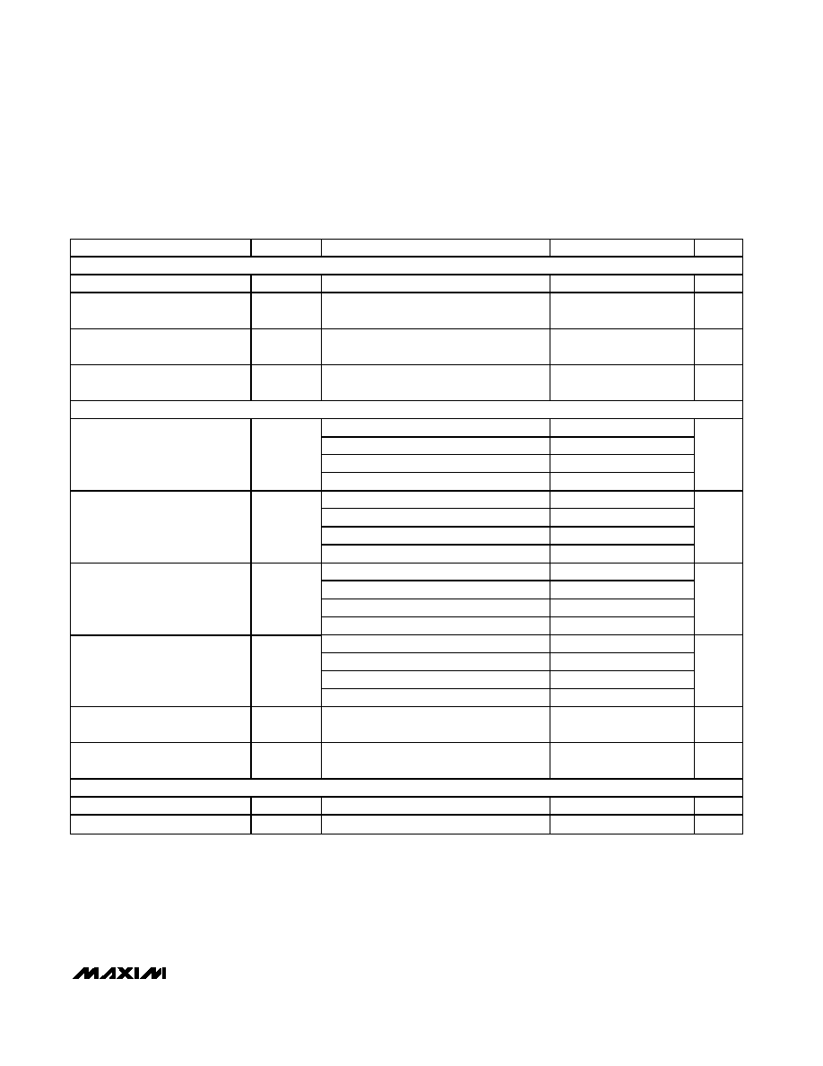
ABSOLUTE MAXIMUM RATINGS
ELECTRICAL CHARACTERISTICS
(AV
CC
= OV
CC
= 1.8V, AGND = OGND = 0, f
SAMPLE
= 170MHz, differential sine-wave clock input drive, 0.1µF capacitor on REFIO,
internal reference, digital output pins differential R
L
= 100
±1%, T
A
= T
MIN
to T
MAX
, unless otherwise noted. Typical values are at
T
A
= +25∞C.) (Note 1)
Stresses beyond those listed under "Absolute Maximum Ratings" may cause permanent damage to the device. These are stress ratings only, and functional
operation of the device at these or any other conditions beyond those indicated in the operational sections of the specifications is not implied. Exposure to
absolute maximum rating conditions for extended periods may affect device reliability.
AV
CC
to AGND ..................................................... -0.3V to +2.1V
OV
CC
to OGND .................................................... -0.3V to +2.1V
AV
CC
to OV
CC
...................................................... -0.3V to +2.1V
AGND to OGND ................................................... -0.3V to +0.3V
INP, INN to AGND ....................................-0.3V to (AV
CC
+ 0.3V)
REFIO, REFADJ to AGND ........................-0.3V to (AV
CC
+ 0.3V)
All Digital Inputs to AGND........................-0.3V to (AV
CC
+ 0.3V)
All Digital Outputs to OGND ....................-0.3V to (OV
CC
+ 0.3V)
ESD on All Pins (Human Body Model) .............................
±2000V
Thermal Resistance (multilayer board)
jc ................................................................................0.8∞C/W
ja .................................................................................24∞C/W
Operating Temperature Range ...........................-40∞C to +85∞C
Junction Temperature .....................................................+150∞C
Storage Temperature Range ............................-60∞C to +150∞C
Maximum Current into Any Pin............................................50mA
Lead Temperature (soldering,10s) ..................................+300∞C
PARAMETER
SYMBOL
CONDITIONS
MIN
TYP
MAX
UNITS
DC ACCURACY
Resolution
12
Bits
Integral Nonlinearity
(Note 2)
INL
f
IN
= 10MHz, T
A
= +25
∞C
-2
±0.75
+2
LSB
Differential Nonlinearity (Note 2)
DNL
T
A
= +25
∞C, No missing codes
-0.8
±0.3
+0.8
LSB
Transfer Curve Offset
V
OS
T
A
= +25
∞C (Note 2)
-3.3
+3.3
mV
Offset Temperature Drift
40
µV/
∞C
ANALOG INPUTS (INP, INN)
Full-Scale Input Voltage Range
V
FS
T
A
= +25
∞C (Note 2)
1320
1454
1590
mV
P-P
Full-Scale Range Temperature
Drift
130
ppm/
∞C
Common-Mode Input Range
V
CM
Internally self-biased
1.365 ±0.15
V
Input Capacitance
C
IN
2.5
pF
Differential Input Resistance
R
IN
3.00
4.2
6.25
k
Full-Power Analog Bandwidth
FPBW
700
MHz
REFERENCE (REFIO, REFADJ)
Reference Output Voltage
V
REFIO
T
A
= +25
∞C, REFADJ = AGND
1.18
1.23
1.30
V
Reference Temperature Drift
90
ppm/
∞C
REFADJ Input High Voltage
V
REFADJ
Used to disable the internal reference
AV
CC
- 0.1
V
SAMPLING CHARACTERISTICS
Maximum Sampling Rate
f
SAMPLE
170
MHz
Minimum Sampling Rate
f
SAMPLE
20
MHz
Clock Duty Cycle
Set by clock-management circuit
40 to 60
%
Aperture Delay
t
AD
Figures 4, 11
620
ps
Aperture Jitter
t
AJ
Figure 11
0.2
ps
RMS
MAX1213
1.8V, 12-Bit, 170Msps ADC for
Broadband Applications
_______________________________________________________________________________________
3
ELECTRICAL CHARACTERISTICS (continued)
(AV
CC
= OV
CC
= 1.8V, AGND = OGND = 0, f
SAMPLE
= 170MHz, differential sine-wave clock input drive, 0.1µF capacitor on REFIO,
internal reference, digital output pins differential R
L
= 100
±1%, T
A
= T
MIN
to T
MAX
, unless otherwise noted. Typical values are at
T
A
= +25∞C.) (Note 1)
PARAMETER
SYMBOL
CONDITIONS
MIN
TYP
MAX
UNITS
CLOCK INPUTS (CLKP, CLKN)
Differential Clock Input Amplitude
(Note 3)
200
500
mV
P-P
Clock Input Common-Mode
Voltage Range
Internally self-biased
1.15 ±0.25
V
Clock Differential Input
Resistance
R
CLK
11
±25%
k
Clock Differential Input
Capacitance
C
CLK
5
pF
DYNAMIC CHARACTERISTICS (at -1dBFS)
f
IN
= 10MHz, T
A
+25∞C
64.5
66.2
f
IN
= 65MHz, T
A
+25∞C
64.5
65.8
f
IN
= 200MHz
65
Signal-to-Noise
Ratio
SNR
f
IN
= 250MHz
64.5
dB
f
IN
= 10MHz, T
A
+25∞C
64
65.9
f
IN
= 65MHz, T
A
+25∞C
63.5
65.2
f
IN
= 200MHz
63.9
Signal-to-Noise
and Distortion
SINAD
f
IN
= 250MHz
63.5
dB
f
IN
= 10MHz, T
A
+25∞C
73
83
f
IN
= 65MHz, T
A
+25∞C
69
76.5
f
IN
= 200MHz
70.7
Spurious-Free
Dynamic Range
SFDR
f
IN
= 250MHz
72.9
dBc
f
IN
= 10MHz, T
A
+25∞C
-85
-73
f
IN
= 65MHz, T
A
+25∞C
-76.5
-69
f
IN
= 200MHz
-70.7
Worst Harmonics
(HD2 or HD3)
f
IN
= 250MHz
-72.9
dBc
Two-Tone Intermodulation
Distortion
TTIMD
f
IN1
= 99MHz at -7dBFS,
f
IN2
= 101MHz at -7dBFS
-78
dBc
Noise Power Ratio
NPR
f
NOTCH
= 28.8MHz
±1MHz,
noise BW = 50MHz, A
IN
= -9.1dBFS
59.5
dB
LVDS DIGITAL OUTPUTS (D0P/N≠D11P/N, ORP/N)
Differential Output Voltage
|V
OD
|
R
L
= 100
±1%
250
400
mV
Output Offset Voltage
OV
OS
R
L
= 100
±1%
1.125
1.310
V

MAX1213
1.8V, 12-Bit, 170Msps ADC for
Broadband Applications
4
_______________________________________________________________________________________
ELECTRICAL CHARACTERISTICS (continued)
(AV
CC
= OV
CC
= 1.8V, AGND = OGND = 0, f
SAMPLE
= 170MHz, differential sine-wave clock input drive, 0.1µF capacitor on REFIO,
internal reference, digital output pins differential R
L
= 100
±1%, T
A
= T
MIN
to T
MAX
, unless otherwise noted. Typical values are at
T
A
= +25∞C.) (Note 1)
PARAMETER
SYMBOL
CONDITIONS
MIN
TYP
MAX
UNITS
LVCMOS DIGITAL INPUTS (CLKDIV,
T/B)
Digital Input Voltage Low
V
IL
0.2 x AV
CC
V
Digital Input Voltage High
V
IH
0.8 x AV
CC
V
TIMING CHARACTERISTICS
CLK-to-Data Propagation Delay
t
PDL
Figure 4
1.75
ns
CLK-to-DCLK Propagation Delay
t
CPDL
Figure 4
4.95
ns
DCLK-to-Data Propagation Delay
t
PDL
- t
CPDL
Figure 4 (Note 3)
2.8
3.2
3.6
ns
LVDS Output Rise Time
t
RISE
20% to 80%, C
L
= 5pF
460
ps
LVDS Output Fall Time
t
FALL
20% to 80%, C
L
= 5pF
460
ps
Output Data Pipeline Delay
t
LATENCY
Figure 4
11
Clock
cycles
POWER REQUIREMENTS
Analog Supply Voltage Range
AV
CC
1.70
1.80
1.90
V
Digital Supply Voltage Range
OV
CC
1.70
1.80
1.90
V
Analog Supply Current
I
AVCC
f
IN
= 65MHz
375
425
mA
Digital Supply Current
I
OVCC
f
IN
= 65MHz
63
75
mA
Analog Power Dissipation
P
DISS
f
IN
= 65MHz
788
900
mW
Offset
1.8
mV/V
Power-Supply Rejection Ratio
(Note 4)
PSRR
Gain
1.5
%FS/V
Note 1:
+25∞C guaranteed by production test, <+25∞C guaranteed by design and characterization.
Note 2: Static linearity and offset parameters are computed from a best-fit straight line through the code transition points. The full-
scale range (FSR) is defined as 4095 x slope of the line.
Note 3: Parameter guaranteed by design and characterization: T
A
= T
MIN
to T
MAX
.
Note 4: PSRR is measured with both analog and digital supplies connected to the same potential.

MAX1213
1.8V, 12-Bit, 170Msps ADC for
Broadband Applications
_______________________________________________________________________________________
5
Typical Operating Characteristics
(AV
CC
= OV
CC
= 1.8V, AGND = OGND = 0, f
SAMPLE
= 170MHz, A
IN
= -1dBFS; see each TOC for detailed information on test condi-
tions, differential input drive, differential sine-wave clock input drive, 0.1µF capacitor on REFIO, internal reference, digital output pins
differential R
L
= 100
, T
A
= +25∞C.)
FFT PLOT
(8192-POINT DATA RECORD)
MAX1213 toc01
ANALOG INPUT FREQUENCY (MHz)
AMPLITUDE (dBFS)
-100
-90
-80
-70
-60
-50
-40
-30
-20
-10
0
-110
HD2
f
SAMPLE
= 170MHz
f
IN
= 12.47192MHz
A
IN
= -1.001dBFS
SNR = 66.7dB
SINAD = 66.4dB
SFDR = 83.8dBc
HD2 = -83.8dBc
HD3 = -84dBc
HD3
70
60
40
50
20
30
10
0
80
FFT PLOT
(8192-POINT DATA RECORD)
MAX1213 toc02
ANALOG INPUT FREQUENCY (MHz)
AMPLITUDE (dBFS)
-100
-90
-80
-70
-60
-50
-40
-30
-20
-10
0
-110
HD2
f
SAMPLE
= 170MHz
f
IN
= 65.09888MHz
A
IN
= -1.099dBFS
SNR = 66.5dB
SINAD = 65.7dB
SFDR = 76dBc
HD2 = -77.7dBc
HD3 = -76dBc
HD3
70
60
40
50
20
30
10
0
80
FFT PLOT
(8192-POINT DATA RECORD)
MAX1213 toc03
ANALOG INPUT FREQUENCY (MHz)
AMPLITUDE (dBFS)
-100
-90
-80
-70
-60
-50
-40
-30
-20
-10
0
-110
HD2
f
SAMPLE
= 170MHz
f
IN
= 200.11108MHz
A
IN
= -1.025dBFS
SNR = 65dB
SINAD = 63.9dB
SFDR = 70.7dBc
HD2 = -74.8dBc
HD3 = -70.7dBc
HD3
70
60
40
50
20
30
10
0
80
FFT PLOT
(8192-POINT DATA RECORD)
MAX1213 toc04
ANALOG INPUT FREQUENCY (MHz)
AMPLITUDE (dBFS)
-100
-90
-80
-70
-60
-50
-40
-30
-20
-10
0
-110
HD2
f
SAMPLE
= 170MHz
f
IN
= 250.04038MHz
A
IN
= -1.040dBFS
SNR = 64.5dB
SINAD = 63.5dB
SFDR = 72.9dBc
HD2 = -77.4dBc
HD3 = -72.9dBc
HD3
70
60
40
50
20
30
10
0
80
TWO-TONE IMD PLOT
(8192-POINT DATA RECORD)
MAX1213 toc05
ANALOG INPUT FREQUENCY (MHz)
AMPLITUDE (dBFS)
-100
-90
-80
-70
-60
-50
-40
-30
-20
-10
0
-110
f
IN2
f
SAMPLE
= 170MHz
f
IN1
= 99.25659MHz
f
IN2
= 101.08276MHz
A
IN1
= A
IN2
= -6.974dBFS
IMD = -78dBc
f
IN1
- f
IN2
f
IN1
+ f
IN2
3f
IN2
- 2f
IN1
2f
IN1
- f
IN2
f
IN1
70
60
40
50
20
30
10
0
80
45
50
60
55
65
70
0
100
50
150
200
250
300
SNR/SINAD vs. ANALOG INPUT FREQUENCY
(f
SAMPLE
= 170MHz, A
IN
= -1dBFS)
MAX1213 toc06
f
IN
(MHz)
SNR/SINAD (dB)
SNR
SINAD
40
45
50
55
60
65
70
75
80
85
90
95
0
50
100
150
200
250
300
SFDR vs. ANALOG INPUT FREQUENCY
(f
SAMPLE
= 170MHz, A
IN
= -1dBFS
MAX1213 toc07
f
IN
(MHz)
SFDR (dBc)
-100
-85
-90
-95
-80
-75
-70
-65
-60
-55
-50
0
100
50
150
200
250
300
HD2/HD3 vs. ANALOG INPUT FREQUENCY
(f
SAMPLE
= 170MHz, A
IN
= -1dBFS)
MAX1213 toc08
f
IN
(MHz)
HD2/HD3 (dBc)
HD3
HD2
10
30
20
50
40
60
70
-55
-45 -40 -35
-50
-30 -25 -20 -15 -10 -5
0
MAX1213 toc09
ANALOG INPUT AMPLITUDE (dBFS)
SNR/SINAD (dB)
SINAD
SNR/SINAD vs. ANALOG INPUT AMPLITUDE
(f
SAMPLE
= 170MHz, f
IN
= 65.098877MHz)
SNR